← Back to Projects
HardwareShipped

Custom Arduino Sensor PCB

First complete PCB: KiCad schematic through two-layer layout and Gerbers for an Arduino Nano, HC-SR04, and status LED.

I built this to learn the real board house pipeline, not to invent a fancy circuit. Custom HC-SR04 footprint from measured dimensions, two-layer routing with a ground plane, DRC, then Gerber and Excellon export for PCBWay. Breadboards were familiar. Owning symbols, copper, mask, and fab files was the point.

Engineering highlights

  • Designed my first complete PCB from schematic capture through fab-ready Gerbers
  • Built a custom KiCad footprint for the HC-SR04 from measured dimensions
  • Routed a two-layer board with ground plane, DRC, and PCBWay export
Date
Summer 2026
Focus
PCB Design
Build stage
Fabrication-ready Gerbers
Disciplines
PCB Design · Electrical Design · Manufacturing Prep
kicadpcbhardwareultrasonicarduinogerber
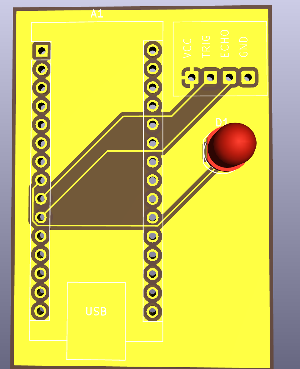
Final 3D render
Final 3D render of the ultrasonic sensor PCB
Full write-up below. The hero is the short version. This is the build story: what I designed, what broke, and why I made the calls I did.

Motivation

Why I started this

What pulled me in, and what I wanted to get better at.

Why I built it

I had only ever built on breadboards. I wanted one complete pass through a real PCB workflow before the next robotics board got complicated.

What interested me

The circuit is intentionally simple. The work is schematic to footprint to two-layer layout to Gerbers you can send out.

What I wanted to learn

Custom libraries, copper layers, plated holes, solder mask, silkscreen, DRC, and a fab package. That pipeline is what I wanted to own.

System Overview

How the system fits together

A compact two-layer through-hole PCB that seats an Arduino Nano, an HC-SR04 ultrasonic sensor on a custom four-pin footprint, a status LED, and the power/signal routing between them. Designed in KiCad and exported as Gerber + Excellon files for PCBWay.

01

Schematic

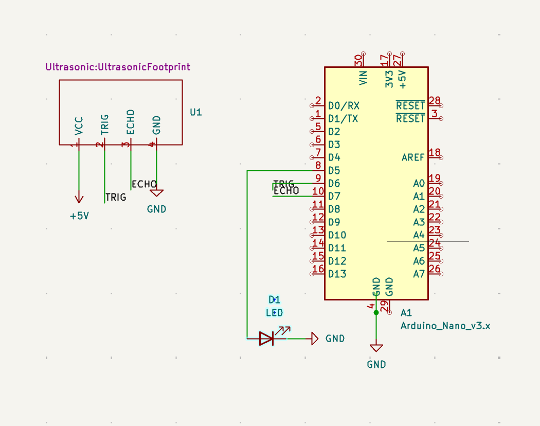
Nano GPIO, power, ultrasonic interface, and LED wired with manufacturable footprints assigned.

02

Custom HC-SR04 library

Symbol and footprint from measured sensor dimensions instead of a wrong generic connector.

03

Two-layer PCB

Signal and power routing, ground plane, DRC-clean layout.

04

Fab package

Gerber layers and Excellon drills ready for commercial fabrication.

Data flow

Ultrasonic echo/trigger pins and LED → Nano GPIO on the board. Power and ground distributed through the copper and ground plane.

Control flow

Firmware can live on the Nano later. This project stops at a board you can fabricate and populate.

Final 3D render
KiCad 3D render of the finished ultrasonic sensor PCB

Fabrication-ready board in KiCad's 3D viewer after routing.

Engineering Breakdown

Broken down by discipline

Each block covers the goal, the design, what broke, what changed, and what shipped.

01Electrical / Schematic

Electrical / Schematic

Goal

Capture a Nano + HC-SR04 + LED circuit with footprints that can actually be manufactured.

Design

Full schematic in KiCad. Power and signal nets to the ultrasonic header and status LED. Every part gets a real footprint before layout starts.

Challenges

  • Generic footprints lie about pin pitch and body size.
  • Easy to leave a net unassigned until DRC or 3D view catches it.

Iterations

  • Breadboard mental model.
  • Schematic with stock parts.
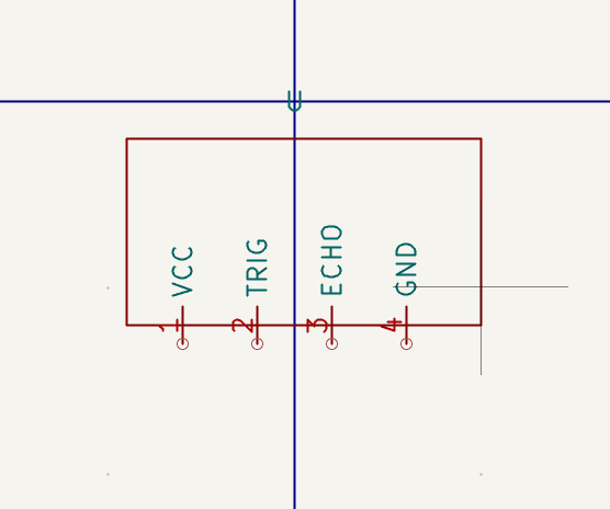
  • Custom HC-SR04 symbol once the stock connector was clearly wrong.

Final implementation

Schematic with Nano, custom ultrasonic symbol, LED, and manufacturable footprints ready for PCB.

Schematic
KiCad schematic for Nano, ultrasonic sensor, and LED

Schematic capture before layout.

02PCB Layout

PCB Layout

Goal

Route a clean two-layer board with a ground plane and a custom sensor footprint that matches the real HC-SR04.

Design

Compact through-hole layout. Custom footprint from measured dimensions. Signal and power traces, then copper pour / ground plane. DRC until the board was legal for fab.

Challenges

  • First time owning copper layers, plated through-holes, mask, and silkscreen as real constraints.
  • Footprint errors only show up when the physical sensor will not sit on the pads.

Iterations

  • Pre-trace placement and 3D check.
  • Routed copper and ground plane.
  • DRC cleanup before export.

Final implementation

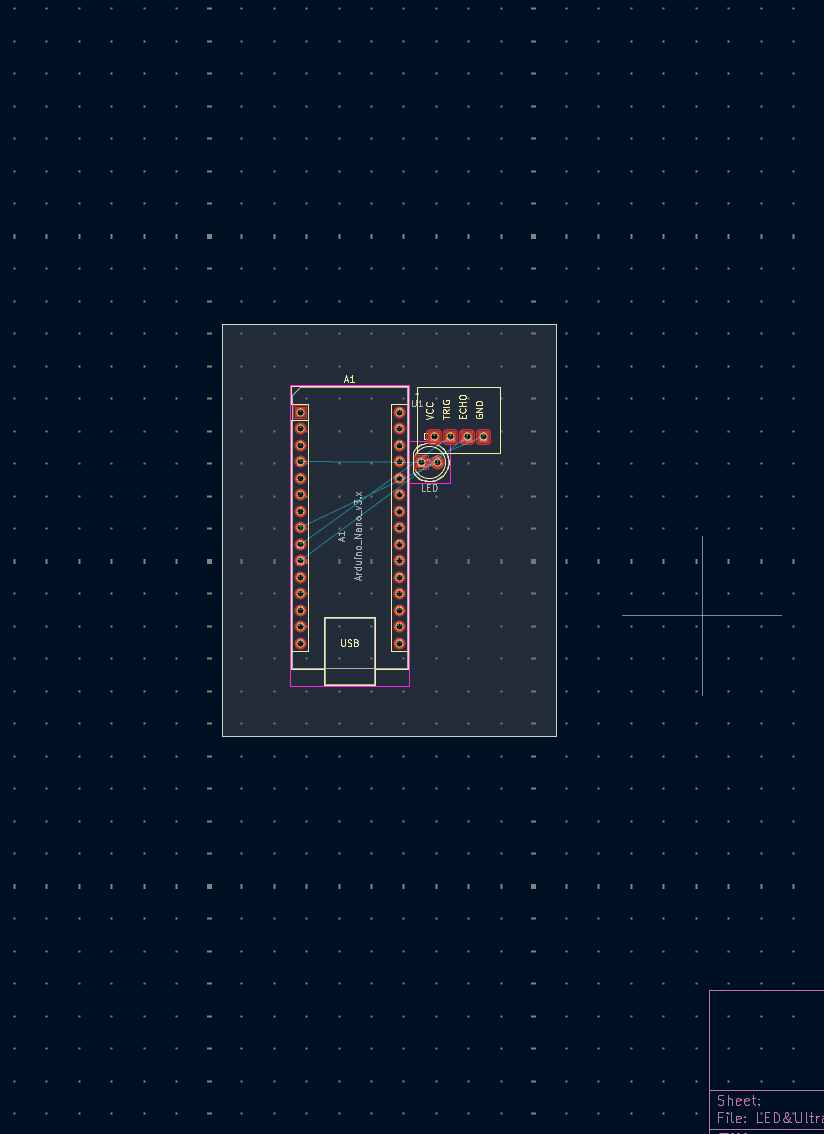
Two-layer routed PCB with custom ultrasonic footprint, ground plane, and DRC-clean design.

PCB editor
KiCad PCB editor view of the routed board

Routed two-layer layout in KiCad.

Custom footprint
Custom HC-SR04 symbol and footprint editor

HC-SR04 library part from measured dimensions.

03Manufacturing Prep

Manufacturing Prep

Goal

Export a fab package a board house can build without guesswork.

Design

Gerber layers plus Excellon drills. Final check in the 3D viewer before packing files for PCBWay.

Challenges

  • Missing a layer or drill file is a silent fab failure.
  • 3D view catches mechanical collisions that DRC does not.

Iterations

  • Pre-trace 3D preview.
  • Post-route 3D and Gerber export.
  • Fab package for PCBWay.

Final implementation

Fabrication-ready Gerber and drill set generated from the finished layout.

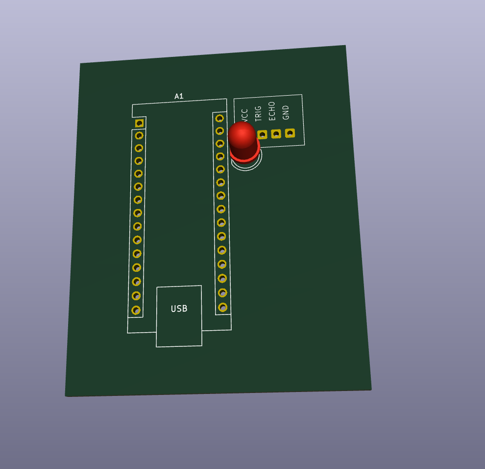
Pre-trace 3D
KiCad 3D render before copper routing

Early 3D check before finishing traces.

Key Design Decisions

Calls I actually made

What else was on the table, what I picked, and why it still made sense once the hardware was real.

01

Keep the circuit simple on purpose

The problem

First PCB: chase features or chase the workflow?

Alternatives considered

  • Dense multi-sensor board
  • Minimal Nano + ultrasonic + LED

Tradeoffs

A denser board looks impressive and hides process mistakes. A small board makes library, layout, and fab mistakes obvious.

Why I chose this

Minimal circuit. Learn the pipeline first.

02

Custom HC-SR04 footprint

The problem

Trust a generic connector footprint or measure the part?

Alternatives considered

  • Stock pin header footprint
  • Custom footprint from calipers

Tradeoffs

Stock is faster until the sensor will not mount. Measuring once beats a respin.

Why I chose this

Custom symbol and footprint from physical dimensions.

03

Through-hole for a first board

The problem

Through-hole or jump straight to SMD?

Alternatives considered

  • SMD-first
  • Through-hole Nano and sensor

Tradeoffs

SMD is denser; through-hole is more forgiving for hand assembly and first-time fab.

Why I chose this

Through-hole so assembly risk stays separate from layout learning.

Evolution

How it got here

Bench bring-up, CAD fits, soldering, and the demos in between. Not just the final photo.

  1. Stage 1

    Schematic

    Nano, ultrasonic, LED nets with footprints assigned.

    Schematic
    Schematic stage
  2. Stage 2

    Custom library + placement

    HC-SR04 footprint and early 3D placement check.

    Placement
    Pre-trace 3D
  3. Stage 3

    Route + Gerbers

    Copper, ground plane, DRC, fab export.

    Final board
    Final routed board

Results & Validation

What held up

What worked in the end, what I can show for it, and where it's still limited.

Custom library parts

Symbol / footprint editor stills

HC-SR04 symbol and footprint built for this board instead of forcing a generic header.

Two-layer routed PCB

PCB editor + final 3D render

Signal routing, power, ground plane, and DRC-clean layout in KiCad.

Fab package

Manufacturing export

Gerber and Excellon files generated for commercial fabrication (PCBWay).

Photos and clips

The runs and stills that match the results above.

Fab-ready board
Final fabrication-ready PCB 3D render

End state of the first complete PCB pass.

Limitations

  • Electrically simple by design; the point was process, not circuit novelty.
  • Physical board bring-up and firmware validation come after fab returns.
  • No public GitHub repo linked yet.

Reflection

Looking back

What surprised me, what I'd redo, and questions I'm still chewing on.

What surprised me

  • Most of the learning was libraries and fab hygiene, not drawing wires.
  • 3D view caught issues DRC was happy to ignore.

What I would redesign

  • Lock mechanical keepouts earlier for the Nano USB and sensor cone.
  • Document a Gerber checklist so export is mechanical next time.

Future improvements

  • Populate and bring up the fabbed board.
  • Reuse this workflow on denser robotics and motor-driver PCBs.

Questions that emerged

  • When does a first board's simplicity stop being discipline and start being avoidance?
  • What should move to SMD once the through-hole fab loop is boring?