Comparator 1
Has the brake signal crossed its required threshold?
Turns an analog brake condition into a clear decision edge for the logic stage.
Designed and analyzed a sensor-monitoring circuit and evaluated buck-converter architectures for an automotive electrical environment.
Independent engineering work for Penn Electric Racing's recruitment process—not PER vehicle hardware. Brake and current thresholds feed comparator and logic stages that drive an indicator under a response-time requirement, while a buck stage is judged on efficiency, headroom, ripple, EMI, and packaging instead of 'outputs 5 V' alone.
Engineering highlights
Motivation
What pulled me in, and what I wanted to get better at.
Why I built it
I wanted to prove I could turn a written electrical requirement into a circuit that monitors sensor thresholds, makes a logic decision, and drives an indicator under real timing and automotive supply constraints.
What interested me
The interesting part was not drawing a schematic. It was deciding how threshold detection, logic, timing, and a 5 V rail from a noisy ~12 V vehicle supply should fit together without inventing convenience that the environment will punish.
What I wanted to learn
I wanted a harder look at buck-converter selection: efficiency, headroom, ripple, EMI, and board area as a system, not as a single 'outputs 5 V' checkbox.
System Overview
Independent engineering work for Penn Electric Racing's recruitment process. The circuit watches brake and current sensor conditions, decides when those conditions are satisfied together, and activates an indicator within a required response window. Power comes from an automotive-style 12 V domain that must be regulated for the sensing and logic stages.
Power regulation
Steps the vehicle supply into a clean enough low-voltage rail for references, comparators, and logic.
Sensor inputs
Bring brake and current sensing into the threshold stage with usable reference levels.
Threshold detection
Comparators answer whether each sensor has crossed its required level.
Logic + timing
Combine conditions and shape the response so the indicator meets the timing requirement.
Indicator
Make the decision visible without loading the decision node incorrectly.
Data flow
12 V supply → regulation → sensor/reference network → comparators → logic → timing → indicator.
Control flow
Analog thresholds become digital decisions; the timing network enforces response behavior before the LED stage.
Design Challenge Deep Dive
Independent engineering work completed as part of Penn Electric Racing's recruitment process. Not hardware designed for or used on the PER car.
Signal / power path
Each stage answers one question. If a block cannot justify itself, it should not be on the board.
Comparator 1
Has the brake signal crossed its required threshold?
Turns an analog brake condition into a clear decision edge for the logic stage.
Comparator 2
Has the current signal crossed its required threshold?
Same idea for current sensing so both conditions share a comparable decision language.
Logic
Are the required conditions simultaneously true?
Prevents an indicator trip on a single sensor event when concurrency is required.
Timing
Does the circuit satisfy the required response behavior?
Shapes how quickly the decision becomes a visible indicator event.
Power regulation
Is the low-voltage rail honest under automotive supply and load?
Keeps references and logic alive without dumping switching pain into the sensing path.
Indicator
Can a human see the decision without loading the circuit badly?
Closes the loop from requirement to observable behavior.
Schematic
TODO: replace with CircuitLab schematic export (schematic.png) in this folder.
Datasheet comparison
Exact numbers left as placeholders until datasheet values are filled in.
| Metric | LM5164 | LMR33630 | Why it matters |
|---|---|---|---|
| Efficiency | TODO · datasheet | TODO · datasheet | Less energy wasted as heat in a packed enclosure. |
| Output-current capability / headroom | TODO · datasheet | TODO · datasheet | Provides margin when MCU, sensors, or CAN circuitry create transient loads. |
| Transient response | TODO · datasheet | TODO · datasheet | Determines how well the 5 V rail stays regulated when load current suddenly changes. |
| Output-voltage ripple | TODO · datasheet | TODO · datasheet | Excessive supply noise can affect sensitive analog measurements. |
| EMI behavior | TODO · datasheet | TODO · datasheet | Fast switching edges can inject noise into nearby sensor and communication circuitry. |
| PCB footprint | TODO · datasheet | TODO · datasheet | Matters in tightly packaged automotive electronics. |
| Thermal behavior | TODO · datasheet | TODO · datasheet | Heat that has nowhere to go becomes a reliability and layout problem. |
Efficiency
Less energy wasted as heat in a packed enclosure.
LM5164
TODO
LMR33630
TODO
Output-current capability / headroom
Provides margin when MCU, sensors, or CAN circuitry create transient loads.
LM5164
TODO
LMR33630
TODO
Transient response
Determines how well the 5 V rail stays regulated when load current suddenly changes.
LM5164
TODO
LMR33630
TODO
Output-voltage ripple
Excessive supply noise can affect sensitive analog measurements.
LM5164
TODO
LMR33630
TODO
EMI behavior
Fast switching edges can inject noise into nearby sensor and communication circuitry.
LM5164
TODO
LMR33630
TODO
PCB footprint
Matters in tightly packaged automotive electronics.
LM5164
TODO
LMR33630
TODO
Thermal behavior
Heat that has nowhere to go becomes a reliability and layout problem.
LM5164
TODO
LMR33630
TODO
Understanding EMI
Radiated EMI
Conducted noise on the supply path
Conducted noise
Switching disturbances travel through PCB traces, supply rails, or ground and show up as rail bounce or reference noise.
Radiated noise
Fast-changing currents and voltages create electromagnetic fields that can couple into nearby circuitry without a shared conductor.
On a sensor / data-acquisition board near electrically noisy drivetrain hardware, both paths matter. A quiet schematic can still become a noisy measurement if the buck stage is treated as isolated from the analog neighborhood.
Verification is where the design meets the written requirement. Waveform first; numbers only when measured.
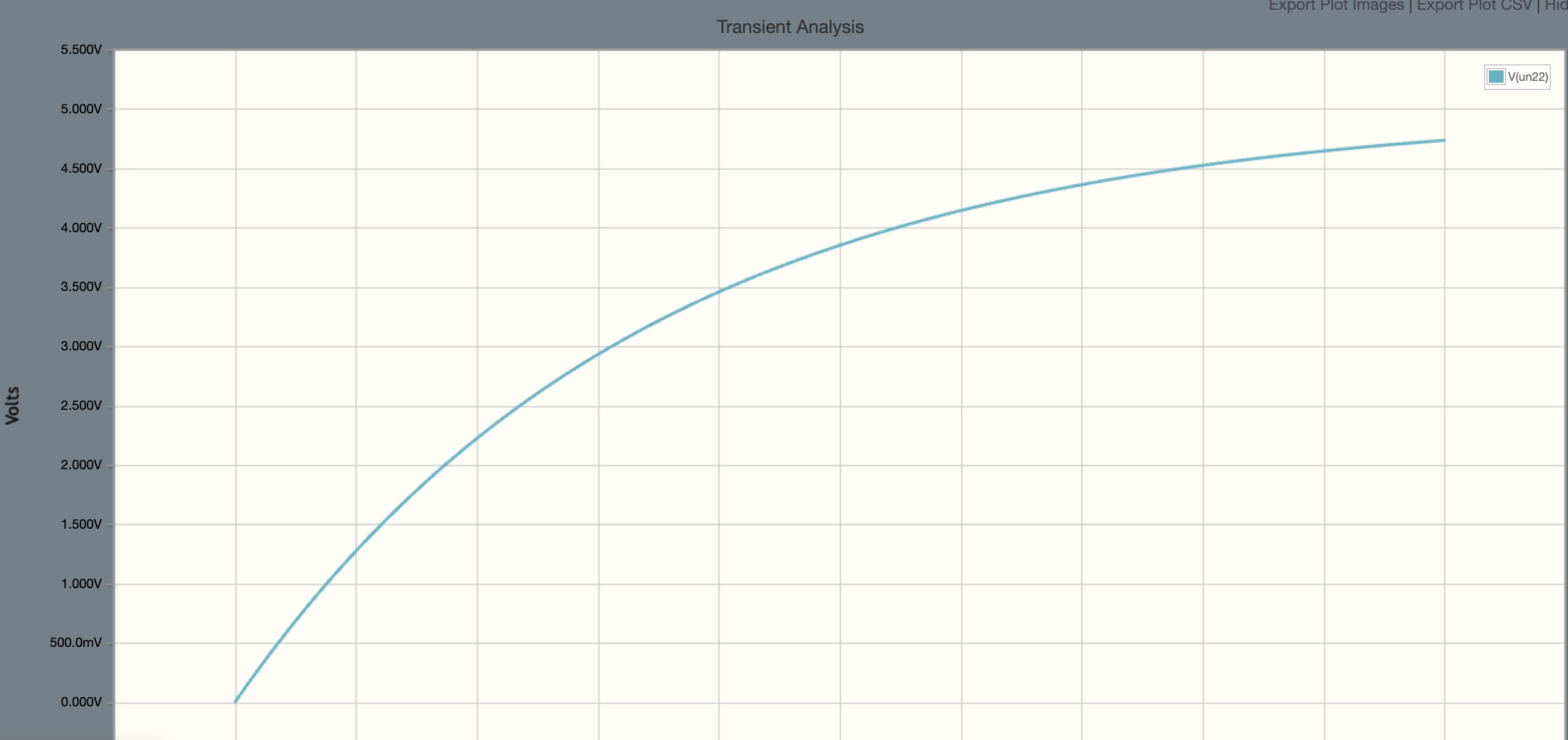
Primary simulation evidence from the challenge submission.
| Requirement | Design mechanism | Verification method | Result |
|---|---|---|---|
| Indicator responds within the allowed response window | Comparator + logic + timing network | CircuitLab transient analysis | TODO · result |
| Both sensor conditions required before indication | Concurrent logic on comparator outputs | Functional simulation / schematic review | TODO · result |
| 5 V rail suitable for sensing/logic under automotive input | Buck regulation stage | Datasheet comparison + (TODO) rail simulation | TODO · result |
Indicator responds within the allowed response window
Mechanism: Comparator + logic + timing network
Method: CircuitLab transient analysis
TODO · result
Both sensor conditions required before indication
Mechanism: Concurrent logic on comparator outputs
Method: Functional simulation / schematic review
TODO · result
5 V rail suitable for sensing/logic under automotive input
Mechanism: Buck regulation stage
Method: Datasheet comparison + (TODO) rail simulation
TODO · result
Engineering was iterative. The circuit could function and still be wrong relative to the written response-time requirement.
Initial interpretation
Treated 0.5 s more like a minimum delay aesthetic than a maximum allowable response.
Simulation
Captured transient behavior for the indicator path.
Compare against the written requirement
Re-read the response-time wording as a bound the design must stay inside.
Identify the mismatch
A 'working' delay story can still fail a maximum-response requirement.
Revise understanding / design
Updated the timing interpretation so verification targets the real constraint.
Engineering Breakdown
Each block covers the goal, the design, what broke, what changed, and what shipped.
Goal
Detect when brake and current conditions are simultaneously satisfied and drive an indicator.
Design
Comparator stages for each threshold, logic that requires the concurrent condition, and a timing network that sets response behavior.
Challenges
Iterations
Final implementation
Comparator + logic + timing path aimed at concurrent detection and bounded indicator response.
Goal
Generate a usable 5 V rail from an automotive ~12–17 V domain without treating the converter as a black box.
Design
Compared candidate buck architectures (LM5164 vs LMR33630 class parts) against efficiency, current headroom, transient behavior, ripple, EMI, footprint, and thermal story.
Challenges
Iterations
Final implementation
Documented selection criteria and comparison scaffold for the buck stage.
Key Design Decisions
What else was on the table, what I picked, and why it still made sense once the hardware was real.
The problem
Generating 5 V from ~12–17 V looks simple until load steps, ripple, EMI, and packaging show up.
Alternatives considered
Tradeoffs
A tiny or cheap part can still heat the board, ring the rail, or couple noise into analog paths.
Why I chose this
Score candidates on system metrics first. Exact datasheet numbers remain TODO placeholders until filled from the sheets.
The problem
An RC timing network can satisfy 'the circuit waits' while still violating a maximum allowable response.
Alternatives considered
Tradeoffs
Misreading the written requirement produces a working waveform that fails the spec.
Why I chose this
Re-check simulation against the requirement text, then revise the timing interpretation.
Evolution
Bench bring-up, CAD fits, soldering, and the demos in between. Not just the final photo.
Draft
Built the sensing → compare → logic → indicate story before locking the power stage.
Simulate
Ran CircuitLab transient analysis to see indicator timing against the intended behavior.
Correct
Caught that the response-time wording was a maximum, not a minimum delay, and revised understanding/design.
Results & Validation
What worked in the end, what I can show for it, and where it's still limited.
CircuitLab transient analysis is on the page as primary verification evidence for response behavior.
Exact measured value still needs to be filled from the simulation readout.
Pass/fail against the written response requirement is left as an explicit TODO so the page never invents a result.
Photos and clips
The runs and stills that match the results above.
CircuitLab transient analysis from the submission package. Read timing from the plot; do not invent numbers here.
Limitations
Reflection
What surprised me, what I'd redo, and questions I'm still chewing on.
What surprised me
What I would redesign
Future improvements
Questions that emerged